
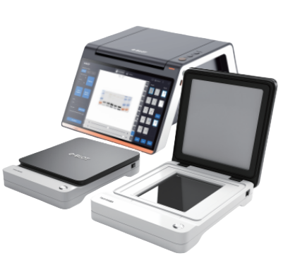
Touch Imager
See the Invisible, Define the Possible
World’s First Direct-Touchlmaging Technology
Specifications
|
Parameter |
Specification |
|
Capture Mode |
Auto / Manual |
|
Full Well Capacity |
2, 500, 000 electrons |
|
Data Transfer Speed |
10, 000 Mbps |
|
Light Sources Control |
Chemiluminescence and Epi-white |
|
Exposure Time |
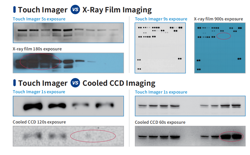
0.1 second to 600 seconds* *Over 95% of imaging is completed within 1 second. |
|
Marker |
Color marker |
|
Photo Sensorchip Dimension |
120 mm × 140 mm (168 cm2) |
|
Imaging Area |
117 mm × 137 mm (≈160.3 cm2) |
|
User Management |
Multi-user management |
|
Net Weight |
4.35 kg |
|
Dimensions (L × W × H) |
270 mm × 206 mm × 54 mm |
|
Power Supply |
100-250 V |
|
Working Temperature |
4-30℃ |
|
Working Humidity |
10-85% relative humidity (non condensing) |
|
Water-Resistant |
IP55 equivalent |
Adopted By 1000+ Research Institutions, 600+ Peer-Reviewed Publications
Large Field of View: 15 μm pixel size, 16 megapixels (4k × 4k)
High-Speed: 24 fps at full resolution, no need for pixel binning to achieve higher imaging speeds, up to 90 fps at 2k×2k resolution.
Image Drift Correction: Effectively compensates for imaging drift, ensuring clarity and enhancing high-resolution image quality.
Video Recording: Facilitates in-situ TEM imaging, capturing dynamic microscopic world.
High-Sensitivity Scintillator : Optimized for 120‒300 kV TEM, with 30 kV customization available.
High Flexibility: Compatible with TEM models from major brands such as Thermo Fisher, JEOL, and Hitachi.
AI-Enhanced: Equipped with an independent high-performance AI workstation, featuring built-in AI modules and algorithm libraries, supporting customized configurations to meet the personalized needs of multiple fields.
Modular Design: Three core modules allow for future upgrades and replacements, offering flexibility, customization, reduced maintenance costs, and minimized downtime.